Self-etch PCB with Tones Transfer
This article describes the way I am etching my pcbs as rapid prototypes.
I started self etching because on one hand I was interessted in learning
to etch PCBs by myself and on the other hand they look more beautiful
than perfboard prototypes. Don't get me wrong: Perfboard circuits are good
if they are easy and can quickly be soldered. I will summarize the preparation,
i.e. the steps you should do in your CAD programm, the transfer method and
the etching process.
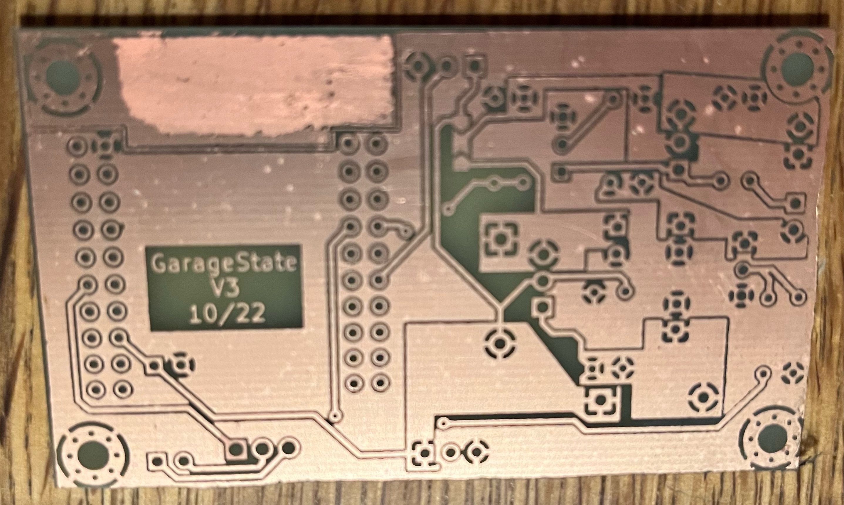
The goal of this process is to produce a single layer PCB with silk screen and
solder mask. The picture below shows a possible result.
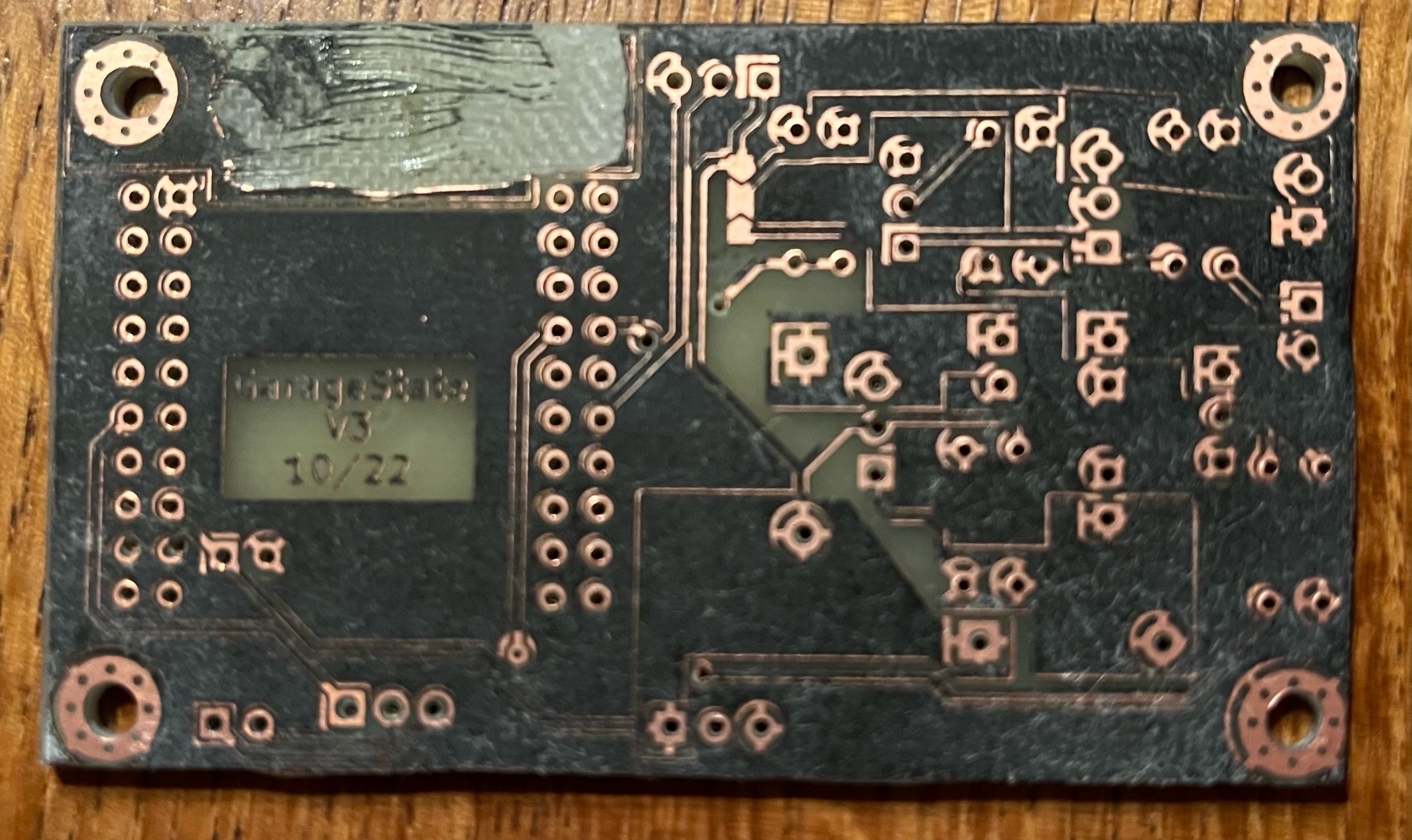
Before you ask: The deformed area on the top of the back side is due to a mistake I made: The PCB includes a ESP32 microcontroller, which has a PCB antenna built in. To prevent the antenna from interferring with my design I should have removed the copper below the antenna. Due to a mistake in my PCB design the copper in this area was keept. I just dremeled it away.
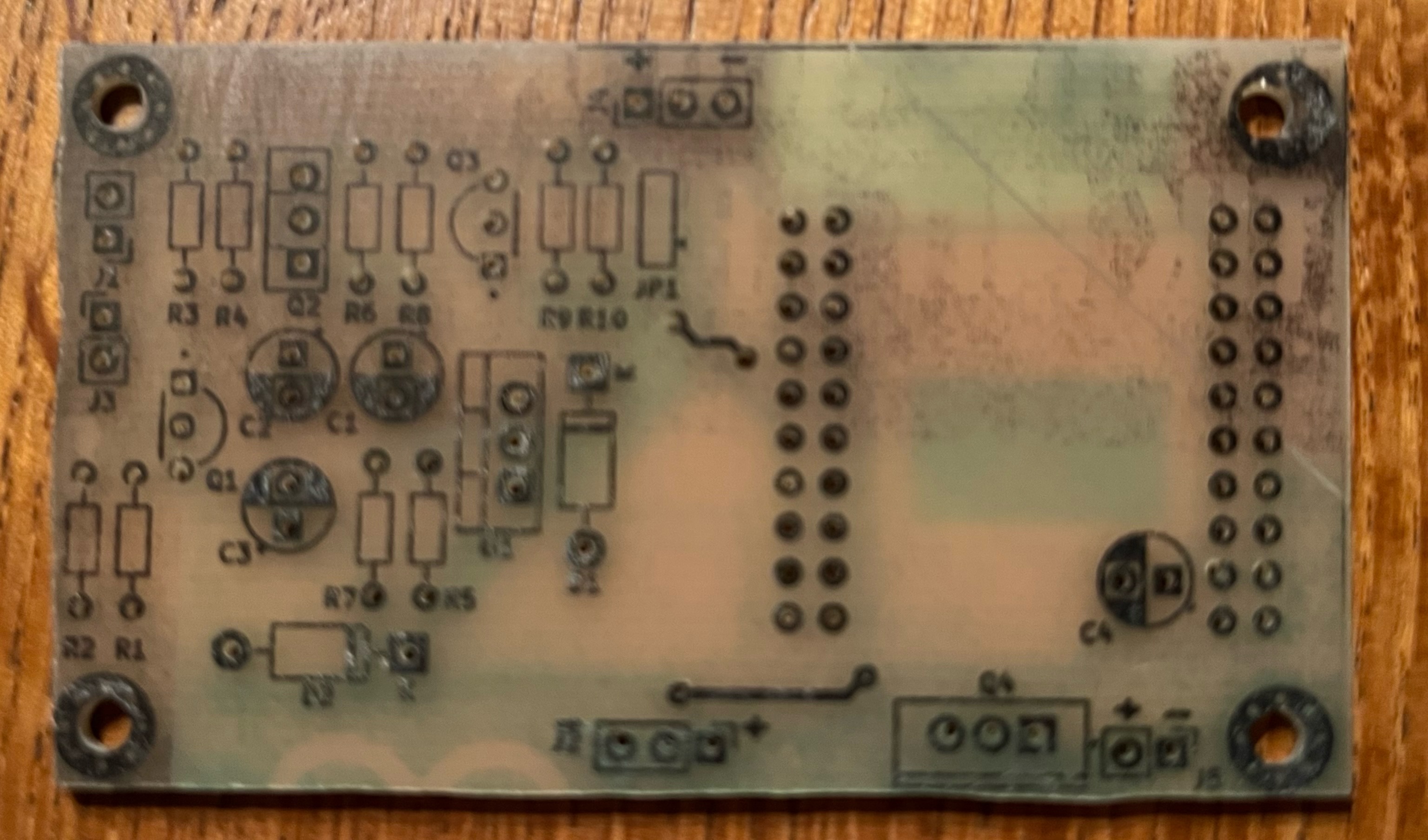
Preparation in CAD
KiCAD is my favorite CAD tool. But you can use any tool you like. Eagle is as
good as Coral Draw as long as the tool supports multiple layers for layouting.
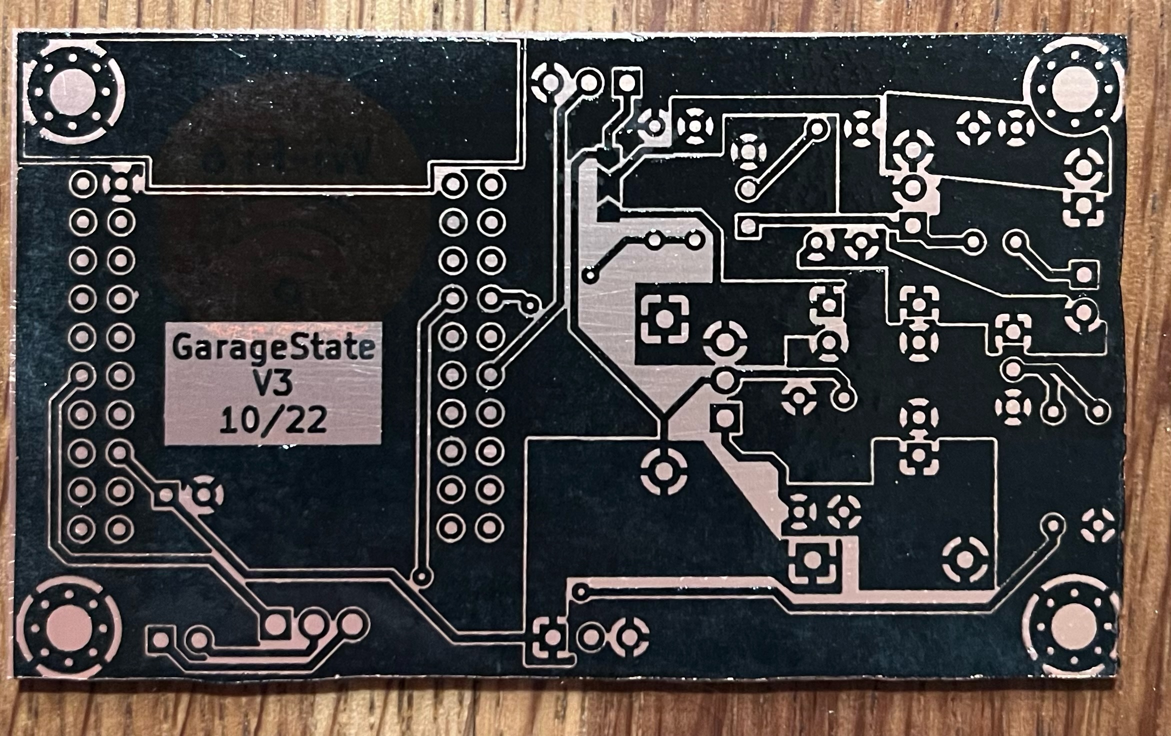
Put your traces on the back layer and your silk screen on the front layer.
Print the back layer with a laser printer. Choose print settings that make the printer
use as much toner as possible. For printing I use a very glossy, very thin paper,
which is often used for magazines or catalogues.
Print two copies of the back layer. On the second print make sure you do not print the vias
and throughhole pads. This second print will be used as solder stop.
The front layer should be printed mirrored.
Make sure that vias and throughhole pads have a radius of 0.8mm in your design. Same
goes for all throughhole pads. I use a diameter of 1.6 mm and a hole size of 0.8mm.
The trace width I set to 0.8mm with a spacing of 0.8 mm.
Tools
You will need:
- An electric iron
- A hard, fire resistant surface for ironing
- A paper tissue
- 10 to 20 ml Aceton for cleaning the PCB
- A plastic bowl, big enough for your PCB
- A single sided PCB
- Enough sodium persulfate (Na2S2O8) to cover the pcb when laying in the bowl
- Toothbrush
- 0.8 mm drill bit
- sandpaper (min 180) or steel wool
Toner Transfer
In this step you need the printed back layer. Cut the print to size and align it
with the PCB with the printed side to the copper side. Heat up your iron. Use a medium set up.
Prepare the hard and fire resistant surface and a tissue. To fix the print on the PCB you can
iron it onto the PCB for 2-3 seconds. Then place it in the tissue and wrap the tissue around it.
If the iron is heated, put the tissue onto the hard surface with the copper side up. Now put the
iron on the PCB for about 2 minutes and put some pressure on it. Change the position every aprox.
30 seconds to make sure pressure is applied on every area of the PCB.
Info
If you change the position, make sure to lift the iron. If you just slide the iron, there is a
danger to smudge the toner.
Etching
Prepare your plastic bowl for etching. Heat up the sodium persulfate to speed up the reaction.
Info
Make sure that the temperature of the sodium persulfate does not exceed 50°C.
Higher temperatures cause a higher desintegration of the sodium persulfate.
Place the PCB in the bowl so that it is fully covered by the sodium persulfate. Keep it in there for about 10 to 15 minutes depending on the temperature and the amount of copper you like to etch. every now and then give it a gentle shake to make sure the sodium persulfate which is in direct contect with the PCB gets washed away. If every copper was etched away, remove the PCB from the bowl and rinse it in the sink.
Info:
Please be aware that sodium persulfate is hazardous to your health and the environment.
So please handly it with care and on your own risk. Do not depollute into the sink. Collect it
and bring it to authorized depollution companies.
Info
You can reuse the sodium persulfate. I used it up to 5 times for etching my PCBs.
I store it in a glass bottle when not in use. But do not fully close the bottle. Sodium persulfate
reacts even in closed bottles. In this case the pressure inside the bottle can make it burst.
Drilling
Use the 0.8mm drill bit to drill holes in the PCB. I use a Dremel drill tool and a self made drill stand.
You surely do not need a drill stand, but it makes things way easier.
After you finished drilling the holes, search the one hole you mnissed. because there always is one hole
you miss. If you are absolutly sure you drilled every hole, smoothen the drill edges with the help of
sandpaper (min 180) or steel wool.
Applying the Silkscreen and Soldermask
Iron the silkscreen as described in chapter Toner Transfer. I usually make the silkscreen stck to the PCB with a short ironing, then turn the PCB over and make the solder mask stick to it on the other side. Once I am sure both print outs are in place and fixed I wrap the PCB in a tissue and iron every side for 2 minutes.
Info
If you made a mistake in the solder mask and it covers more than needed, you can easily
remove parts of it with the help of aceton.
Last edit: 2022-11-27
