How I built my own esp32 dev board
It all started with Digikey offering some ESP32-WROOM-32UE modules with a good discount. I was interested in building my own development board since quite a while. The project to build with this controller was easily identified: A infrared reader for smart electrical meters. But before I startet with the IR reader, I wanted to build a simpler board to learn how to build such a board. I wanted to build the board as cheap as possible, so I just used components I had laying around on my bench. It is not the most beauftiful board ever made, but it works.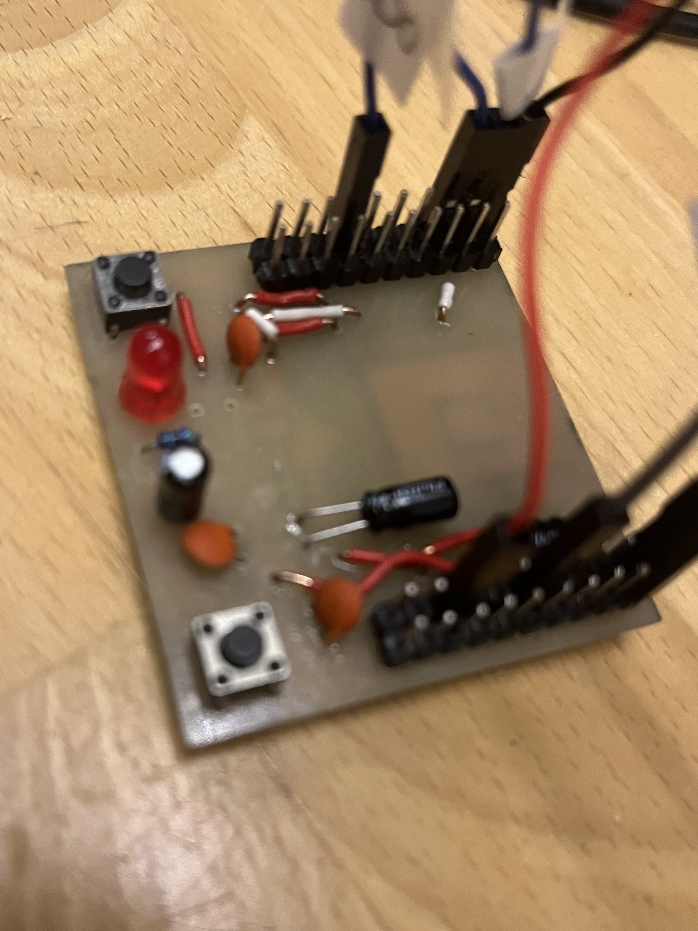
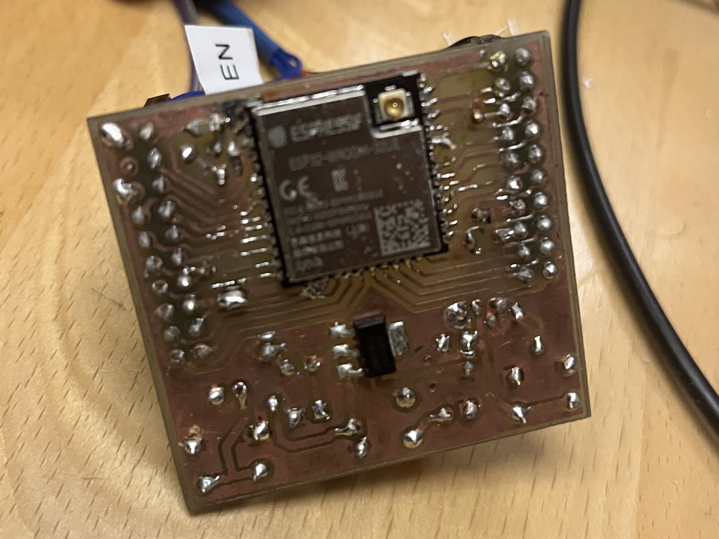
As you can see, I used some through hole components I had laying around and I needed to route some traces on the top side of the board. Yes, I realized that using male pin headers and through hole caps on the same side it a rather stupid idea. at least I realized once I tried to push that thing into a solderless breadboard. On the back side I celebrated my premier of hand soldering a 0805 capacitor and even a 0603 resistor. Once done I was surprised how easy it was.
Espressif is very kind and published areference design for their devkitc on their website which gives you all necessary details to create a schematic in the CAD tool of your choice. I preffer to use KiCAD. you can see my design here
Following Espressif's reference design I used a TS1117 LDO regulator, which is a drop in replacement of the AMS1117 Espressif uses.
It is able to delivery up to 800 mA and a stable output voltage of 3.3V. I picked the SOT-223 package, which seemed easier solderable
than the SO-8 housing.
To be able to flash the board or just reset it, I added two switches for pulling the enable pin or the boot pin to ground.
 Once the design was finished and the PCB layed out, I etched the PCB like I already described in my article about
PCB etching. I mainly designed for a single side PCB, but some routings required a second side. It took me four attempts to etch this board as the smallest
trace width is 0.3 mm, which is in my opinion the s,allest trace you can etch in this hobbiest way I do it. I needed those thin traces to route the controller pads
to the plugs. To have enough headroom between trace and plug pad I needed to go down to 0.3 mm.
Once the design was finished and the PCB layed out, I etched the PCB like I already described in my article about
PCB etching. I mainly designed for a single side PCB, but some routings required a second side. It took me four attempts to etch this board as the smallest
trace width is 0.3 mm, which is in my opinion the s,allest trace you can etch in this hobbiest way I do it. I needed those thin traces to route the controller pads
to the plugs. To have enough headroom between trace and plug pad I needed to go down to 0.3 mm.
Last edit: 2023-09-24
